- 您现在的位置:买卖IC网 > Sheet目录2003 > LTC1400IS8 (Linear Technology)IC A/D CONV 12BIT W/SHTDN 8-SOIC
LTC1400
3
1400fa
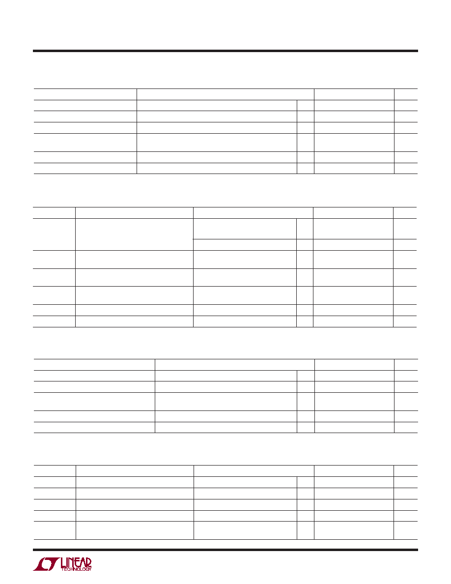
PARAMETER
CONDITIONS
MIN
TYP
MAX
UNITS
Resolution (No Missing Codes)
●
12
Bits
Integral Linearity Error
(Note 9)
●
±1
LSB
Differential Linearity Error
●
±1
LSB
Offset Error
(Note 10)
●
±6
±8
LSB
Full-Scale Error
±15
LSB
Full-Scale Tempco
IOUT(REF) = 0
●
±10
±45
ppm/°C
CO VERTER CHARACTERISTICS
U
The ● denotes the specications which apply over the full operating
temperature range, otherwise specications are at TA = 25°C unless otherwise noted. With internal reference (Notes 5, 8)
PARAMETER
CONDITIONS
MIN
TYP
MAX
UNITS
VREF Output Voltage
IOUT = 0
2.400
2.420
2.440
V
VREF Output Tempco
IOUT = 0
●
±10
±45
ppm/°C
VREF Load Regulation
4.75V ≤ VCC ≤ 5.25V
–5.25V ≤ VSS ≤ 0V
0.01
LSB/V
VREF Load Regulation
0 ≤ |IOUT| ≤ 1mA
2
LSB/mA
VREF Wake-Up Time from Sleep Mode (Note 7) CVREF = 10μF
4
ms
I TER AL REFERE CE CHARACTERISTICS
U
The ● denotes the specications which apply over the
full operating temperature range, otherwise specications are at TA = 25°C unless otherwise noted. (Note 5)
SYMBOL
PARAMETER
CONDITIONS
MIN
TYP
MAX
UNITS
S/(N + D)
Signal-to-Noise
Plus Distortion Ratio
100kHz Input Signal
Commercial
Industrial
●
70
69
72
dB
200kHz Input Signal
72
dB
THD
Total Harmonic Distortion
Up to 5th Harmonic
100kHz Input Signal
200kHz Input Signal
●
–82
–80
–76
dB
Peak Harmonic or
Spurious Noise
100kHz Input Signal
200kHz Input Signal
●
–84
–82
–76
dB
IMD
Intermodulation Distortion
fIN1 = 99.51kHz, fIN2 = 102.44kHz
fIN1 = 199.12kHz, fIN2 = 202.05kHz
–82
–70
dB
Full Power Bandwidth
4
MHz
Full Linear Bandwidth (S/(N + D) ≥ 68dB)
900
kHz
DY A IC ACCURACY
U
W
The ● denotes the specications which apply over the full operating temperature range,
otherwise specications are at TA = 25°C. VCC = 5V, VSS = –5V, fSAMPLE = 400kHz unless otherwise noted. (Note 5)
DIGITAL I PUTS A D DIGITAL OUTPUTS
U
The ● denotes the specications which apply over the
full operating temperature range, otherwise specications are at TA = 25°C unless otherwise noted. (Note 5)
SYMBOL
PARAMETER
CONDITIONS
MIN
TYP
MAX
UNITS
VIH
High Level Input Voltage
VCC = 5.25V
●
2.0
V
VIL
Low Level Input Voltage
VCC = 4.75V
●
0.8
V
IIN
Digital Input Current
VIN = 0V to VCC
●
±10
μA
CIN
Digital Input Capacitance
5
pF
VOH
High Level Output Voltage
VCC = 4.75V, IO = –10μA
VCC = 4.75V, IO = –200μA
●
4.0
4.7
V
发布紧急采购,3分钟左右您将得到回复。
相关PDF资料
LTC1401IS8#TRPBF
IC A/D CONV 12BIT W/SHTDN 8-SOIC
LTC1402IGN#TRPBF
IC ADC 12BIT 2.2MSPS SHDN 16SSOP
LTC1403AHMSE#TRPBF
IC ADC 14BIT 2.8MSPS DIFF 10MSOP
LTC1403AIMSE-1#TRPBF
IC ADC 14BIT 2.8MSPS DIFF 10MSOP
LTC1404IS8#TRPBF
IC A/D CONV 12BIT W/SHTDN 8-SOIC
LTC1405IGN#TRPBF
IC ADC 12BIT 5MSPS SAMPLE 28SSOP
LTC1406IGN#TRPBF
IC A/D CONV 8BIT SAMPLING 24SSOP
LTC1407AHMSE#PBF
IC ADC 14BIT 3MSPS 10-MSOP
相关代理商/技术参数
LTC1400IS8#PBF
功能描述:IC A/D CONV 12BIT W/SHTDN 8-SOIC RoHS:是 类别:集成电路 (IC) >> 数据采集 - 模数转换器 系列:- 标准包装:1 系列:microPOWER™ 位数:8 采样率(每秒):1M 数据接口:串行,SPI? 转换器数目:1 功率耗散(最大):- 电压电源:模拟和数字 工作温度:-40°C ~ 125°C 安装类型:表面贴装 封装/外壳:24-VFQFN 裸露焊盘 供应商设备封装:24-VQFN 裸露焊盘(4x4) 包装:Digi-Reel® 输入数目和类型:8 个单端,单极 产品目录页面:892 (CN2011-ZH PDF) 其它名称:296-25851-6
LTC1400IS8#TR
功能描述:IC ADC 12BIT 400KSPS SHTDN 8SOIC RoHS:否 类别:集成电路 (IC) >> 数据采集 - 模数转换器 系列:- 标准包装:1,000 系列:- 位数:16 采样率(每秒):45k 数据接口:串行 转换器数目:2 功率耗散(最大):315mW 电压电源:模拟和数字 工作温度:0°C ~ 70°C 安装类型:表面贴装 封装/外壳:28-SOIC(0.295",7.50mm 宽) 供应商设备封装:28-SOIC W 包装:带卷 (TR) 输入数目和类型:2 个单端,单极
LTC1400IS8#TRPBF
功能描述:IC A/D CONV 12BIT W/SHTDN 8-SOIC RoHS:是 类别:集成电路 (IC) >> 数据采集 - 模数转换器 系列:- 标准包装:1,000 系列:- 位数:16 采样率(每秒):45k 数据接口:串行 转换器数目:2 功率耗散(最大):315mW 电压电源:模拟和数字 工作温度:0°C ~ 70°C 安装类型:表面贴装 封装/外壳:28-SOIC(0.295",7.50mm 宽) 供应商设备封装:28-SOIC W 包装:带卷 (TR) 输入数目和类型:2 个单端,单极
LTC1400IS8PBF
制造商:Linear Technology 功能描述:ADC SAR 400ksps 12-Bit Serial SOIC8
LTC1401CS8
功能描述:IC A/D CONV 12BIT W/SHTDN 8-SOIC RoHS:否 类别:集成电路 (IC) >> 数据采集 - 模数转换器 系列:- 标准包装:2,500 系列:- 位数:16 采样率(每秒):15 数据接口:MICROWIRE?,串行,SPI? 转换器数目:1 功率耗散(最大):480µW 电压电源:单电源 工作温度:-40°C ~ 85°C 安装类型:表面贴装 封装/外壳:38-WFQFN 裸露焊盘 供应商设备封装:38-QFN(5x7) 包装:带卷 (TR) 输入数目和类型:16 个单端,双极;8 个差分,双极 配用:DC1011A-C-ND - BOARD DELTA SIGMA ADC LTC2494
LTC1401CS8#PBF
功能描述:IC A/D CONV 12BIT W/SHTDN 8-SOIC RoHS:是 类别:集成电路 (IC) >> 数据采集 - 模数转换器 系列:- 标准包装:1 系列:microPOWER™ 位数:8 采样率(每秒):1M 数据接口:串行,SPI? 转换器数目:1 功率耗散(最大):- 电压电源:模拟和数字 工作温度:-40°C ~ 125°C 安装类型:表面贴装 封装/外壳:24-VFQFN 裸露焊盘 供应商设备封装:24-VQFN 裸露焊盘(4x4) 包装:Digi-Reel® 输入数目和类型:8 个单端,单极 产品目录页面:892 (CN2011-ZH PDF) 其它名称:296-25851-6
LTC1401CS8#TR
功能描述:IC ADC 12BIT 200KSPS SHTDN 8SOIC RoHS:否 类别:集成电路 (IC) >> 数据采集 - 模数转换器 系列:- 标准包装:2,500 系列:- 位数:16 采样率(每秒):15 数据接口:MICROWIRE?,串行,SPI? 转换器数目:1 功率耗散(最大):480µW 电压电源:单电源 工作温度:-40°C ~ 85°C 安装类型:表面贴装 封装/外壳:38-WFQFN 裸露焊盘 供应商设备封装:38-QFN(5x7) 包装:带卷 (TR) 输入数目和类型:16 个单端,双极;8 个差分,双极 配用:DC1011A-C-ND - BOARD DELTA SIGMA ADC LTC2494
LTC1401CS8#TRPBF
功能描述:IC A/D CONV 12BIT W/SHTDN 8-SOIC RoHS:是 类别:集成电路 (IC) >> 数据采集 - 模数转换器 系列:- 标准包装:2,500 系列:- 位数:16 采样率(每秒):15 数据接口:MICROWIRE?,串行,SPI? 转换器数目:1 功率耗散(最大):480µW 电压电源:单电源 工作温度:-40°C ~ 85°C 安装类型:表面贴装 封装/外壳:38-WFQFN 裸露焊盘 供应商设备封装:38-QFN(5x7) 包装:带卷 (TR) 输入数目和类型:16 个单端,双极;8 个差分,双极 配用:DC1011A-C-ND - BOARD DELTA SIGMA ADC LTC2494